- 您现在的位置:买卖IC网 > Sheet目录3894 > PIC16F722A-I/SS (Microchip Technology)MCU PIC 3.5K FLASH XLP 28-SSOP
PIC16(L)F722A/723A
DS41417B-page 22
2010-2012 Microchip Technology Inc.
2.2.2.1
STATUS Register
The STATUS register, shown in Register 2-1, contains:
the arithmetic status of the ALU
the Reset status
the bank select bits for data memory (SRAM)
The STATUS register can be the destination for any
instruction, like any other register. If the STATUS
register is the destination for an instruction that affects
the Z, DC or C bits, then the write to these three bits is
disabled. These bits are set or cleared according to the
device logic. Furthermore, the TO and PD bits are not
writable. Therefore, the result of an instruction with the
STATUS register as destination may be different than
intended.
For example, CLRF STATUS will clear the upper three
bits and set the Z bit. This leaves the STATUS register
as ‘000u u1uu’ (where u = unchanged).
It is recommended, therefore, that only BCF, BSF,
SWAPF and MOVWF instructions are used to alter the
STATUS register, because these instructions do not
affect any Status bits. For other instructions not
affecting any Status bits (Refer to Section 21.0
Note 1: The C and DC bits operate as Borrow
and Digit Borrow out bits, respectively, in
subtraction.
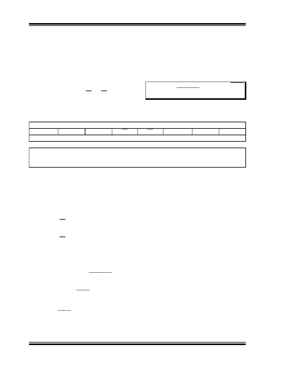
REGISTER 2-1:
STATUS: STATUS REGISTER
R/W-0
R-1
R/W-x
IRP
RP1
RP0
TO
PD
ZDC(1)
C(1)
bit 7
bit 0
Legend:
R = Readable bit
W = Writable bit
U = Unimplemented bit, read as ‘0’
-n = Value at POR
‘1’ = Bit is set
‘0’ = Bit is cleared
x = Bit is unknown
bit 7
IRP: Register Bank Select bit (used for indirect addressing)
1 = Bank 2, 3 (100h-1FFh)
0 = Bank 0, 1 (00h-FFh)
bit 6-5
RP<1:0>: Register Bank Select bits (used for direct addressing)
00 = Bank 0 (00h-7Fh)
01 = Bank 1 (80h-FFh)
10 = Bank 2 (100h-17Fh)
11 = Bank 3 (180h-1FFh)
bit 4
TO: Time-out bit
1 = After power-up, CLRWDT instruction or SLEEP instruction
0 = A WDT time-out occurred
bit 3
PD: Power-down bit
1 = After power-up or by the CLRWDT instruction
0 = By execution of the SLEEP instruction
bit 2
Z: Zero bit
1 = The result of an arithmetic or logic operation is zero
0 = The result of an arithmetic or logic operation is not zero
bit 1
DC: Digit Carry/Digit Borrow bit (ADDWF, ADDLW,SUBLW,SUBWF instructions)(1)
1 = A carry-out from the 4th low-order bit of the result occurred
0 = No carry-out from the 4th low-order bit of the result
bit 0
C: Carry/Borrow bit(1) (ADDWF, ADDLW, SUBLW, SUBWF instructions)(1)
1 = A carry-out from the Most Significant bit of the result occurred
0 = No carry-out from the Most Significant bit of the result occurred
Note 1:
For Borrow, the polarity is reversed. A subtraction is executed by adding the two’s complement of the
second operand. For rotate (RRF, RLF) instructions, this bit is loaded with either the high-order or low-order
bit of the source register.
发布紧急采购,3分钟左右您将得到回复。
相关PDF资料
PIC17LC762T-08/PT
IC MCU OTP 8KX16 A/D PWM 80TQFP
PIC17LC762T-08/L
IC MCU OTP 8KX16 A/D PWM 84PLCC
PIC16F1823-I/SL
IC MCU 8BIT FLASH 14SOIC
PIC17LC762T-08I/PT
IC MCU OTP 8KX16 A/D PWM 80TQFP
PIC17LC762T-08I/L
IC MCU OTP 8KX16 A/D PWM 84PLCC
PIC17LC762-08/PT
IC MCU OTP 8KX16 A/D PWM 80TQFP
PIC17LC762-08I/PT
IC MCU OTP 8KX16 A/D PWM 80TQFP
PIC12LF1822-I/SN
IC MCU 8BIT FLASH 8SOIC
相关代理商/技术参数
PIC16F722AT-I/ML
功能描述:8位微控制器 -MCU 3.5KB Flsh 1.8V-5.5V 16 MHz int Osc RoHS:否 制造商:Silicon Labs 核心:8051 处理器系列:C8051F39x 数据总线宽度:8 bit 最大时钟频率:50 MHz 程序存储器大小:16 KB 数据 RAM 大小:1 KB 片上 ADC:Yes 工作电源电压:1.8 V to 3.6 V 工作温度范围:- 40 C to + 105 C 封装 / 箱体:QFN-20 安装风格:SMD/SMT
PIC16F722AT-I/MV
功能描述:8位微控制器 -MCU 3.5KB Flsh 1.8V-5.5V 16 MHz int Osc RoHS:否 制造商:Silicon Labs 核心:8051 处理器系列:C8051F39x 数据总线宽度:8 bit 最大时钟频率:50 MHz 程序存储器大小:16 KB 数据 RAM 大小:1 KB 片上 ADC:Yes 工作电源电压:1.8 V to 3.6 V 工作温度范围:- 40 C to + 105 C 封装 / 箱体:QFN-20 安装风格:SMD/SMT
PIC16F722AT-I/SO
功能描述:8位微控制器 -MCU 3.5KB Flsh 1.8V-5.5V 16 MHz int Osc RoHS:否 制造商:Silicon Labs 核心:8051 处理器系列:C8051F39x 数据总线宽度:8 bit 最大时钟频率:50 MHz 程序存储器大小:16 KB 数据 RAM 大小:1 KB 片上 ADC:Yes 工作电源电压:1.8 V to 3.6 V 工作温度范围:- 40 C to + 105 C 封装 / 箱体:QFN-20 安装风格:SMD/SMT
PIC16F722AT-I/SS
功能描述:8位微控制器 -MCU 3.5KB Flsh 1.8V-5.5V 16 MHz int Osc RoHS:否 制造商:Silicon Labs 核心:8051 处理器系列:C8051F39x 数据总线宽度:8 bit 最大时钟频率:50 MHz 程序存储器大小:16 KB 数据 RAM 大小:1 KB 片上 ADC:Yes 工作电源电压:1.8 V to 3.6 V 工作温度范围:- 40 C to + 105 C 封装 / 箱体:QFN-20 安装风格:SMD/SMT
PIC16F722-E/ML
功能描述:8位微控制器 -MCU 35 KB Flash 18V-55V 16 MHz Int Osc RoHS:否 制造商:Silicon Labs 核心:8051 处理器系列:C8051F39x 数据总线宽度:8 bit 最大时钟频率:50 MHz 程序存储器大小:16 KB 数据 RAM 大小:1 KB 片上 ADC:Yes 工作电源电压:1.8 V to 3.6 V 工作温度范围:- 40 C to + 105 C 封装 / 箱体:QFN-20 安装风格:SMD/SMT
PIC16F722-E/MV
功能描述:8位微控制器 -MCU 3.5KB Flash 1.8V-5.5V RoHS:否 制造商:Silicon Labs 核心:8051 处理器系列:C8051F39x 数据总线宽度:8 bit 最大时钟频率:50 MHz 程序存储器大小:16 KB 数据 RAM 大小:1 KB 片上 ADC:Yes 工作电源电压:1.8 V to 3.6 V 工作温度范围:- 40 C to + 105 C 封装 / 箱体:QFN-20 安装风格:SMD/SMT
PIC16F722-E/SO
功能描述:8位微控制器 -MCU 35 KB Flash 18V-55V 16 MHz Int Osc RoHS:否 制造商:Silicon Labs 核心:8051 处理器系列:C8051F39x 数据总线宽度:8 bit 最大时钟频率:50 MHz 程序存储器大小:16 KB 数据 RAM 大小:1 KB 片上 ADC:Yes 工作电源电压:1.8 V to 3.6 V 工作温度范围:- 40 C to + 105 C 封装 / 箱体:QFN-20 安装风格:SMD/SMT
PIC16F722-E/SP
功能描述:8位微控制器 -MCU 35 KB Flash 18V-55V 16 MHz Int Osc RoHS:否 制造商:Silicon Labs 核心:8051 处理器系列:C8051F39x 数据总线宽度:8 bit 最大时钟频率:50 MHz 程序存储器大小:16 KB 数据 RAM 大小:1 KB 片上 ADC:Yes 工作电源电压:1.8 V to 3.6 V 工作温度范围:- 40 C to + 105 C 封装 / 箱体:QFN-20 安装风格:SMD/SMT